 RS72X.pdf
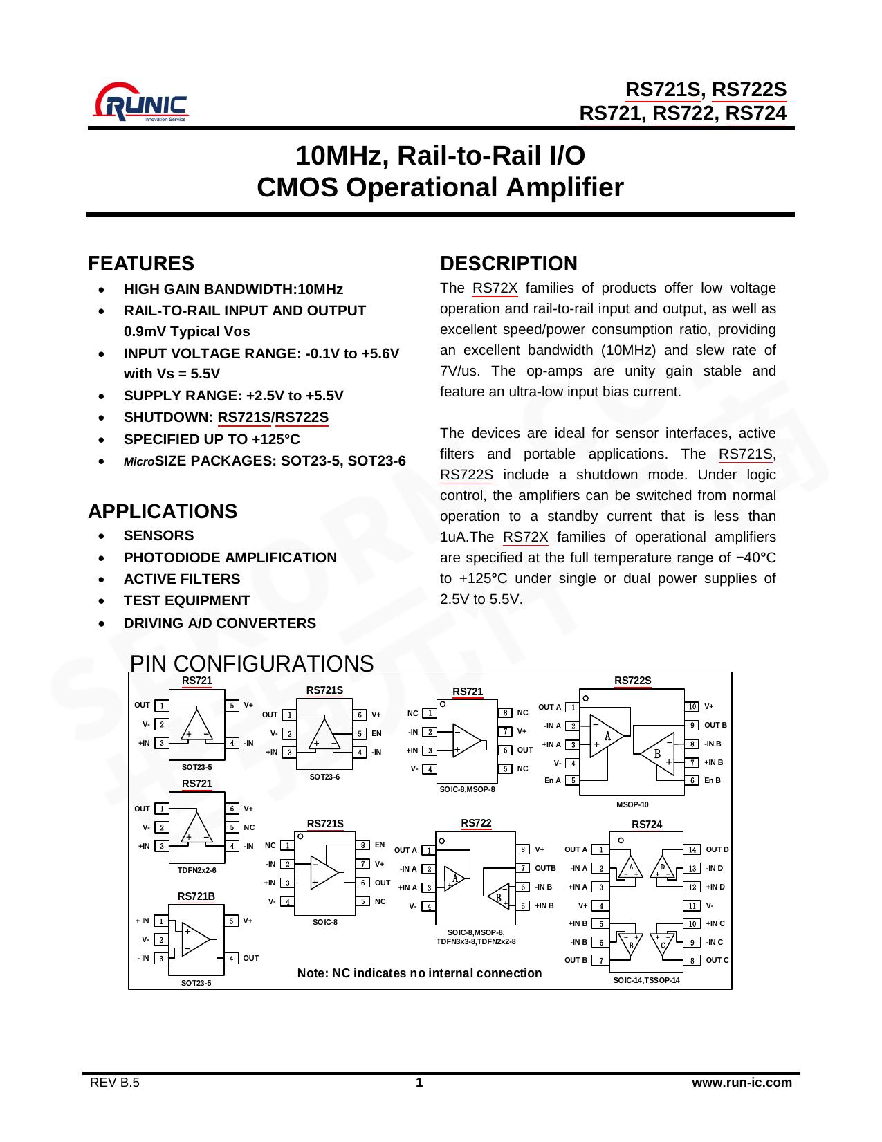
RS72X.pdf
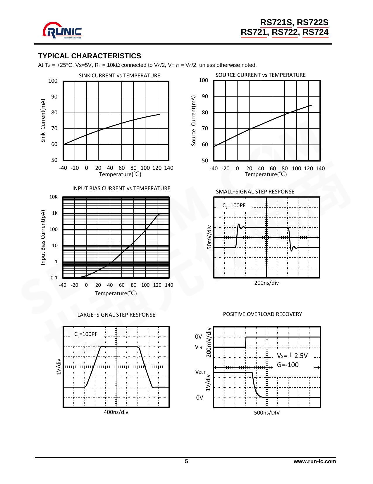
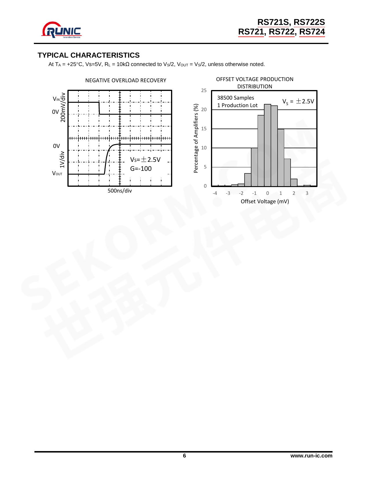
RS721S, RS722S RS721, RS722, RS724 10MHz, Rail-to-Rail I/O CMOS Operational Amplifier FEATURES DESCRIPTION • HIGH GAIN BANDWIDTH:10MHz • RAIL-TO-RAIL INPUT AND OUTPUT 0.9mV Typical Vos • INPUT VOLTAGE RANGE: -0.1V to +5.6V with Vs = 5.5V • SUPPLY RANGE: +2.5V to +5.5V • SHUTDOWN: RS721S/RS722S • SPECIFIED UP TO +125°C • MicroSIZE The RS72X families of products offer low voltage operation and rail-to-rail input and output, as well as excellent speed/power consumption ratio, providing an excellent bandwidth (10MHz) and slew rate of 7V/us. The op-amps are unity gain stable and feature an ultra-low input bias current. The devices are ideal for sensor interfaces, active filters and portable applications. The RS721S, RS722S include a shutdown mode. Under logic control, the amplifiers can be switched from normal operation to a standby current that is less than 1uA.The RS72X families of operational amplifiers are specified at the full temperature range of −40°C to +125°C under single or dual power supplies of 2.5V to 5.5V. PACKAGES: SOT23-5, SOT23-6 APPLICATIONS • SENSORS • PHOTODIODE AMPLIFICATION • ACTIVE FILTERS • TEST EQUIPMENT • DRIVING A/D CONVERTERS PIN CONFIGURATIONS 2 +IN 3 V+ OUT + - V4 5 2 -IN +IN 6 1 3 + - 4 V+ EN -IN SOT23-5 +IN 3 + - 5 NC 4 -IN TDFN2x2-6 RS721B 1 V- 2 - IN 3 5 REV B.5 1 -IN A 2 +IN A 3 V- 4 En A 5 V+ OUT NC - 10 V+ 9 OUT B - 8 -IN B 7 +IN B 6 En B 14 OUT D A B MSOP-10 V+ RS722 NC 1 -IN 2 +IN 3 V- 4 8 EN 7 V+ 6 OUT 5 NC OUT A RS724 8 1 -IN A 2 +IN A 3 V- 4 + A B+ V+ A D OUTB -IN A 2 13 -IN D -IN B +IN A 3 12 +IN D 5 +IN B V+ 4 11 V- +IN B 5 10 +IN C 9 -IN C 8 OUT C OUT Note: NC indicates no internal connection 1 1 6 SOIC-8,MSOP-8, TDFN3x3-8,TDFN2x2-8 4 OUT A 7 SOIC-8 SOT23-5 6 5 4 RS721S + + IN 3 7 OUT A V+ + 2 2 NC SOIC-8,MSOP-8 - V- +IN V- 6 1 -IN 8 1 SOT23-6 RS721 OUT NC + V- 5 - 1 RS721 + OUT RS722S RS721S + RS721 -IN B 6 OUT B 7 - + - + B + - + C SOIC-14,TSSOP-14 www.run-ic.com RS721S, RS722S RS721, RS722, RS724 ABSOLUTE MAXIMUM RATINGS (1) Supply Voltage, V+ to V-...............................................7.0V Input Terminals, Voltage (2) …………... – 0.5 to (V+) + 0.5V Current (2)…………………....…..... ±10mA Storage Temperature ……….…………… −65°C to +150°C Operating Temperature ……….………… −40°C to +125°C Junction Temperature................................................150°C Package Thermal Resistance @ TA = +25°C SOT23-5, SOT23-6………………….………………200°C/W MSOP-10, SOIC-8 …………………….…………... 150°C/W SOIC-14, TSSOP-14……….….….….…..…………100°C/W Lead Temperature (Soldering, 10s) ……………........260°C ESD Susceptibility HBM …......................................................................5000V MM ……………………….........………………...……….400V ESD SENSITIVITY CAUTION ESD damage can range from subtle performance degradation to complete device failure. Precision integrated circuits may be more susceptible to damage because very small parametric changes could cause the device not to meet its published specifications. (1) Stresses above these ratings may cause permanent damage. Exposure to absolute maximum conditions for extended periods may degrade device reliability. These are stress ratings only, and functional operation of the device at these or any other conditions beyond those specified is not implied. (2) Input terminals are diode-clamped to the power-supply rails. Input signals that can swing more than 0.5V beyond the supply rails should be current-limited to 10mA or less. PACKAGE/ORDERING INFORMATION PRODUCT RS721 RS721S RS722 RS722S RS724 TEMPERATURE PACKAGE PACKAGE RANGE LEAD MARKING RS721XK -40℃~125℃ SOIC-8 RS721 Tape and Reel,2500 RS721XF -40℃~125℃ SOT23-5 721 Tape and Reel,3000 RS721BXF -40℃~125℃ SOT23-5 721B Tape and Reel,3000 RS721XM -40℃~125℃ MSOP-8 RS721 Tape and Reel,3000 RS721XTDE6 -40℃~125℃ TDFN2x2-6 721 Tape and Reel,3000 RS721SXK -40℃~125℃ SOIC-8 RS721S Tape and Reel,2500 RS721SXH -40℃~125℃ SOT23-6 721S Tape and Reel,3000 RS722XK -40℃~125℃ SOIC-8 RS722 Tape and Reel,2500 RS722XM -40℃~125℃ MSOP-8 RS722 Tape and Reel,3000 RS722XTDC8 -40℃~125℃ TDFN3x3-8 RS722 Tape and Reel,3000 RS722XTDE8 -40℃~125℃ TDFN2x2-8 RS722 Tape and Reel,3000 RS722SXN -40℃~125℃ MSOP-10 RS722S Tape and Reel,3000 RS724XP -40℃~125℃ SOIC -14 RS724 Tape and Reel,2500 RS724XQ -40℃~125℃ TSSOP-14 RS724 Tape and Reel,3000 ORDERING NUMBER 2 PACKAGE OPTION www.run-ic.com RS721S, RS722S RS721, RS722, RS724 ELECTRICAL CHARACTERISTICS (At TA = +25C, Vs=5V, RL = 10kΩ connected to VS/2, and VOUT = VS/2, unless otherwise noted.) PARAMETER CONDITIONS TJ RS721S,RS722S, RS721,RS722,RS724 MIN TYP MAX UNIT POWER SUPPLY Vs IQ 25°C Operating Voltage Range Quiescent Current/Amplifier PSRR Power-Supply Rejection Ratio 2.5 25°C 25°C Vs= 2.5V to 5.5V Vcm =(V-)+0.5V –40°C to 125°C 1.15 75 5.5 V 1.4 mA 85 dB 65 INPUT Vos Input Offset Voltage 25°C Vos TC Input Offset Voltage Average Drift -40°C to 125°C IB Input Bias Current Ios Input Offset Current Vcm Common-Mode Voltage Range CMRR Common-Mode Rejection Ratio 0.5 2.5 2.6 mV uV/°C 25°C 1 10 pA 25°C 1 10 pA 5.6 V Vs=5.5V 25°C -0.1 Vs = 5.5V, Vcm =-0.1V to 4V 25°C 73 –40°C to 125°C 67 Vs = 5.5V, Vcm = -0.1V to 5.6V 25°C 60 –40°C to 125°C 57 RL =2KΩ, Vo = 0.15V to 4.85V 25°C 86 –40°C to 125°C 65 25°C RL = 10kΩ, Vo = 0.05V to 4.95V –40°C to 125°C 90 85 dB 75 OUTPUT AOL Open-Loop Voltage Gain dB 96 66 25°C 25°C 52 7 mV 25°C 70 mA Slew Rate Gain-Bandwidth Product 25°C 7 V/us 25°C 10 MHz Phase Margin 25°C 62 ° 0.2 us 0.35 us Output Swing From Rail Iout RL = 2KΩ RL = 10kΩ 95 Output Short-Circuit Current FREQUENCY RESPONSE SR GBP Φm ts Settling Time, 0.1% Overload Recovery Time V IN • Gain ≥ V s NOISE en Input-Referred Voltage Noise f = 1 kHz 25°C 9.5 nV/√Hz f = 10 kHz 25°C 6.5 nV/√Hz 25°C <1 uA 25°C 3 us ENABLE/SHUTTDOWN(RS721S,RS722S) IQ(OFF) Supply Current in Shutdown t OFF t ON 25°C 20 us VL Shut Down 25°C V− (V-)+0.8 V VH Amplifier Is Active 25°C (V-)+2 V+ V 3 www.run-ic.com RS721S, RS722S RS721, RS722, RS724 TYPICAL CHARACTERISTICS At TA = +25C, Vs=5V, RL = 10kΩconnected to VS/2, VOUT = VS/2, unless otherwise noted. COMMON−MODE REJECTION RATIO vs FREQUENCY OPEN−LOOP GAIN AND PHASE vs FREQUENCY 120 160 Gain 120 100 60 80 40 60 20 40 0 100 CMRR(dB) Phase 80 Phase Margin (°) Open-Loop Gain(dB) 100 120 140 80 60 40 20 -20 0 10 1K 100K 20 10M 1 1K INPUT VOLTAGE NOISE SPECTRAL DENSITY vs FREQUENCY POWER−SUPPLY REJECTION RATIO vs FREQUENCY 10K 120 | PSRR(dB) 100 10 80 60 40 1 20 10 100 1K 10K 100K 1 10 Frequency(Hz) 100 1K 10K Frequency(KHz) Vs=5V QUIESCENT CURRENT vs TEMPERATURE QUIESCENT CURRENT vs TEMPERATURE 1.3 1.6 1.5 Quiescent Current(mA) Quiescent Current(mA) 100 Frequency(KHz) Vs=5V 100 Voltage Noise (nV/√Hz) 10 Frequency(Hz) 1.4 1.3 1.2 1.1 1 0.9 1.2 1.1 1 0.9 0.8 0.8 -40 -20 0 -40 -20 20 40 60 80 100 120 140 Temperature(℃) Vs=2.7V 4 0 20 40 60 80 100 120 140 Temperature(℃) Vs=5V www.run-ic.com RS721S, RS722S RS721, RS722, RS724 TYPICAL CHARACTERISTICS At TA = +25C, Vs=5V, RL = 10kΩconnected to VS/2, VOUT = VS/2, unless otherwise noted. SINK CURRENT vs TEMPERATURE SOURCE CURRENT vs TEMPERATURE 100 90 Source Current(mA) Sink Current(mA) 100 80 70 60 50 90 80 70 60 50 -40 -20 0 20 40 60 80 100 120 140 Temperature(℃) -40 -20 INPUT BIAS CURRENT vs TEMPERATURE 0 20 40 60 80 100 120 140 Temperature(℃) SMALL−SIGNAL STEP RESPONSE 10K 50mV/div 100 10 1 0.1 -40 -20 0 20 40 60 200ns/div 80 100 120 140 Temperature(℃) POSITIVE OVERLOAD RECOVERY CL=100PF 200mV/div LARGE−SIGNAL STEP RESPONSE 0V VIN 1V/div VS=±2.5V G=-100 VOUT 1V/div Input Bias Current(pA) CL=100PF 1K 0V 400ns/div 500ns/DIV 5 www.run-ic.com RS721S, RS722S RS721, RS722, RS724 TYPICAL CHARACTERISTICS At TA = +25C, Vs=5V, RL = 10kΩconnected to VS/2, VOUT = VS/2, unless otherwise noted. NEGATIVE OVERLOAD RECOVERY Percentage of Amplifiers (%) 0V 25 200mV/div VIN 1V/div 0V VOUT VS=±2.5V G=-100 OFFSET VOLTAGE PRODUCTION DISTRIBUTION 38500 Samples 1 Production Lot 20 VS = ±2.5V 15 10 5 0 500ns/div -4 -3 -2 -1 0 1 2 3 Offset Voltage (mV) 6 www.run-ic.com RS721S, RS722S RS721, RS722, RS724 APPLICATION NOTES The RS721, RS722, RS724, RS721S, RS722S are high precision, rail-to-rail operational amplifiers that can be run from a single-supply voltage 2.5V to 5.5V (±1.25V to ±2.75V). Supply voltages higher than 7V (absolute maximum) can permanently damage the amplifier. +Vs 10uF 0.1uF Vin Rail-to-rail input and output swing significantly increases dynamic range, especially in low-supply applications. Vip Vout RS72X 10uF 0.1uF Good layout practice mandates use of a 0.1uF capacitor place closely across the supply pins. -Vs RS721S/RS722S ENABLE FUNCTION Figure1. Amplifier with Bypass Capacitors The RS721S/RS722S includes a shutdown mode. Under logic control, the amplifiers can be switched from normal mode to a standby current of 1uA. When the Enable pin is connected to high, the amplifier is active. Connecting Enable low disables the amplifier, and places the amplifier, and place the output in a high-impedance state. INSTRUMENTATION AMPLIFIER In the three-op amp, instrumentation amplifier configuration shown in Figure2, V1 LAYOUT GUIDELINS RS72X Attention to good layout practices is always recommended. Keep traces short. When possible, use a PCB ground plane with surface-mount components placed as close to the device pins as possible. Place a 0.1uF capacitor closely across the supply pins. These guidelines should be applied throughout the analog circuit to improve performance and provide benefits such as reducing the EMI susceptibility. RS72X VOUT RS72X V2 Figure2. Amplifier instrumentation amplifier 7 www.run-ic.com RS721S, RS722S RS721, RS722, RS724 PACKAGE OUTLINE DIMENSIONS SOT23-5 D 1.90 b 2.59 E1 E 0.99 0.95 0.69 e e1 RECOMMENDED LAND PATTERN (Unit: mm) 0.2 A A2 L A1 Symbol c θ Dimensions In Millimeters Dimensions In Inches Min Max Min Max A 1.050 1.250 0.041 0.049 A1 0.000 0.100 0.000 0.004 A2 1.050 1.150 0.041 0.045 b 0.300 0.500 0.012 0.020 c 0.100 0.200 0.004 0.008 D 2.820 3.020 0.111 0.119 E 1.500 1.700 0.059 0.067 E1 2.650 2.950 0.104 0.116 e 0.950(BSC) 0.037(BSC) e1 1.800 2.000 0.071 0.079 L 0.300 0.600 0.012 0.024 θ 0° 8° 0° 8° 8 www.run-ic.com RS721S, RS722S RS721, RS722, RS724 SOT23-6 D 1.90 b 2.59 E E1 0.99 Pin1 Index Area 0.95 0.69 e e1 RECOMMENDED LAND PATTERN (Unit: mm) 0.2 A A2 L A1 Symbol c θ Dimensions In Millimeters Dimensions In Inches Min Max Min Max A 1.050 1.250 0.041 0.049 A1 0.000 0.100 0.000 0.004 A2 1.050 1.150 0.041 0.045 b 0.300 0.500 0.012 0.020 c 0.100 0.200 0.004 0.008 D 2.820 3.020 0.111 0.119 E 1.500 1.700 0.059 0.067 E1 2.650 2.950 0.104 0.116 e 0.950(BSC) 0.037(BSC) e1 1.800 2.000 0.071 0.079 L 0.300 0.600 0.012 0.024 θ 0° 8° 0° 8° 9 www.run-ic.com RS721S, RS722S RS721, RS722, RS724 MSOP-8 b e E E1 4.8 1.02 D 0.65 0.41 RECOMMENDED LAND PATTERN (Unit: mm) A2 c A A1 L Symbol Dimensions In Millimeters θ Dimensions In Inches Min Max Min Max A 0.820 1.100 0.032 0.043 A1 0.020 0.150 0.001 0.006 A2 0.750 0.950 0.030 0.037 b 0.250 0.380 0.010 0.015 c 0.090 0.230 0.004 0.009 D 2.900 3.100 0.114 0.122 e 0.650(BSC) 0.026(BSC) E 2.900 3.100 0.114 0.122 E1 4.750 5.050 0.187 0.199 L 0.400 0.800 0.016 0.031 θ 0° 6° 0° 6° 10 www.run-ic.com RS721S, RS722S RS721, RS722, RS724 MSOP-10 b e E 4.65 E1 1.02 0.31 D 0.5 RECOMMENDED LAND PATTERN (Unit: mm) A2 A1 Symbol A c L Dimensions In Millimeters θ Dimensions In Inches Min Max Min Max A 0.820 1.100 0.032 0.043 A1 0.020 0.150 0.001 0.006 A2 0.750 0.950 0.030 0.037 b 0.180 0.280 0.007 0.011 c 0.090 0.230 0.004 0.009 D 2.900 3.100 0.114 0.122 e 0.50(BSC) 0.020(BSC) E 2.900 3.100 0.114 0.122 E1 4.750 5.050 0.187 0.199 L 0.400 0.800 0.016 0.031 θ 0° 6° 0° 6° 11 www.run-ic.com RS721S, RS722S RS721, RS722, RS724 TSSOP-14 e b 5.6 E1 E 1.78 D 0.65 0.42 RECOMMENDED LAND PATTERN (Unit: mm) A2 A A1 Symbol H C θ L Dimensions In Millimeters Min Max A Dimensions In Inches Min Max 1.200 0.047 A1 0.050 0.150 0.002 0.006 A2 0.800 1.050 0.031 0.041 b 0.190 0.300 0.007 0.012 c 0.090 0.200 0.004 0.008 D 4.860 5.100 0.191 0.201 E 4.300 4.500 0.169 0.177 E1 6.250 6.550 0.246 0.258 e L 0.650(BSC) 0.500 H θ 0.026(BSC) 0.700 0.020 0.25(TYP) 1° 0.028 0.01(TYP) 7° 12 1° 7° www.run-ic.com RS721S, RS722S RS721, RS722, RS724 SOIC-8 b e 5.2 E E1 2.2 D 1.27 0.6 RECOMMENDED LAND PATTERN (Unit: mm) A2 c A A1 L Symbol Dimensions In Millimeters θ Dimensions In Inches Min Max Min Max A 1.350 1.750 0.053 0.069 A1 0.100 0.250 0.004 0.010 A2 1.350 1.550 0.053 0.061 b 0.330 0.510 0.013 0.020 c 0.170 0.250 0.007 0.010 D 4.800 5.000 0.189 0.197 e 1.270(BSC) 0.050(BSC) E 5.800 6.200 0.228 0.244 E1 3.800 4.000 0.150 0.157 L 0.400 1.270 0.016 0.050 θ 0° 8° 0° 8° 13 www.run-ic.com RS721S, RS722S RS721, RS722, RS724 SOIC-14 e b 5.2 1.27 E E1 0.6 D 1.27 RECOMMENDED LAND PATTERN (Unit: mm) A2 A1 A c θ L Symbol Dimensions In Millimeters Dimensions In Inches Min Max Min Max A 1.350 1.750 0.053 0.069 A1 0.100 0.250 0.004 0.010 A2 1.350 1.550 0.053 0.061 b 0.310 0.510 0.012 0.020 c 0.100 0.250 0.004 0.010 D 8.450 8.850 0.333 0.348 e 1.270(BSC) 0.050(BSC) E 5.800 6.200 0.228 0.244 E1 3.800 4.000 0.150 0.157 L 0.400 1.270 0.016 0.050 θ 0° 8° 0° 8° 14 www.run-ic.com RS721S, RS722S RS721, RS722, RS724 TDFN3x3-8 E b D E1 L e D1 BOTTOM VIEW A1 A2 A TOP VIEW SIDE VIEW Symbol Dimensions In Millimeters Dimensions In Inches Min Max Min Max A 0.700 0.800 0.028 0.031 A1 0.000 0.050 0.000 0.002 A2 0.203 0.008 b 0.300 0.400 0.012 0.016 D 2.900 3.100 0.114 0.122 D1 2.510 2.610 0.099 0.103 E 2.900 3.100 0.114 0.122 E1 1.550 1.650 0.061 0.065 e L 0.650 TYP 0.350 0.026 TYP 0.450 15 0.014 0.018 www.run-ic.com RS721S, RS722S RS721, RS722, RS724 TDFN2x2-8 E e D E1 L b D1 TOP VIEW BOTTOM VIEW 0.50 0.70 A1 1.95 A2 A 0.65 0.24 1.20 SIDE VIEW RECOMMENDED LAND PATTERN (Unit: mm) Symbol Dimensions In Millimeters Dimensions In Inches Min Max Min Max A 0.700 0.800 0.028 0.031 A1 0.000 0.050 0.000 0.002 A2 0.203(TYP) 0.008(TYP) b 0.180 0.300 0.007 0.012 D 1.900 2.100 0.075 0.083 D1 1.100 1.300 0.043 0.051 E 1.900 2.100 0.075 0.083 E1 0.600 0.800 0.024 0.031 e L 0.500(TYP) 0.250 0.020(TYP) 0.450 16 0.010 0.018 www.run-ic.com RS721S, RS722S RS721, RS722, RS724 TDFN2x2-6 E e D L b 3 TOP VIEW 1 BOTTOM VIEW 0.40 A1 1.95 A2 A 0.65 0.65 SIDE VIEW RECOMMENDED LAND PATTERN (Unit: mm) Symbol Dimensions In Millimeters Dimensions In Inches Min Max Min Max A 0.700 0.800 0.028 0.031 A1 0.000 0.050 0.000 0.002 A2 0.203(TYP) 0.008(TYP) b 0.250 0.350 0.010 0.012 D 1.900 2.100 0.075 0.083 E 1.900 2.100 0.075 0.083 e L 0.650(TYP) 0.250 0.026(TYP) 0.400 17 0.010 0.018 www.run-ic.com